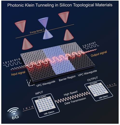
Image: PIB / JNCASR — artistic illustration of photonic Klein tunnelling in a silicon valley photonic crystal chip (official release image).
TL;DR — JNCASR terahertz silicon chip 6G explained: researchers at India's Jawaharlal Nehru Centre for Advanced Scientific Research have built a silicon chip that sends terahertz waves straight through an engineered barrier with only 1–2% signal loss, while carrying data at up to 100 gigabits per second — a step toward compact circuits for future 6G networks.
📌 KEY HIGHLIGHTS
- The result: terahertz waves crossed an engineered barrier in a silicon chip with only about 1–2% loss for a single barrier and 2–3% for two in sequence.
- The speed: the team's power-splitter device carried 100 Gbit/s using QAM-32 modulation — fast enough, in principle, to transfer a 5 GB high-definition film in under half a second.
- The trick: "photonic Klein tunnelling" in a silicon valley photonic crystal whose structure mimics the honeycomb lattice of graphene.
- Who did it: Dr Abhishek Kumar's Meta Optics Laboratory (MetoLab) at JNCASR, with collaborators from IISER Kolkata, IIT Bombay, A*STAR Singapore and the University of Lille/CNRS, France.
- Where it is published: the journal Advanced Materials (DOI: 10.1002/adma.75322), announced by the Press Information Bureau on 4 November 2026.
What happened?
Future sixth-generation (6G) wireless networks are expected to use terahertz frequencies — the band that lies between microwaves and infrared light — because it offers far more bandwidth than today's mobile spectrum. The catch is plumbing: guiding terahertz waves through compact circuits is hard, because bends, junctions and abrupt changes in a waveguide scatter or reflect part of the signal, weakening it as it travels.
Researchers at the Jawaharlal Nehru Centre for Advanced Scientific Research (JNCASR), an autonomous institute of India's Department of Science and Technology, attacked that problem with topological photonics. By arranging triangular holes in a carefully designed pattern in a silicon slab, they created a photonic crystal that guides terahertz waves along the boundary between two regions. Such boundary channels resist certain kinds of backscattering — but a practical circuit must also tolerate deliberately introduced obstacles and changes in geometry. That is what this work demonstrates: the waves kept going even when the team put a barrier in their path.
JNCASR terahertz silicon chip 6G explained: how the barrier trick works
The chip is a silicon photonic crystal whose structure mimics the honeycomb lattice of graphene. The team created a barrier simply by changing the sizes of the triangular holes over a short section of the waveguide. The effect is called photonic Klein tunnelling: the wave passes through the barrier almost as if it were not there.
Two details make this more than a curiosity. First, transmission stayed close to its barrier-free level as long as the barrier strength stayed below a characteristic coupling strength of the crystal — and because the barrier is set by hole geometry, that gives engineers a practical design rule for building such devices. Second, the devices were fabricated on high-resistivity silicon, a material compatible with established semiconductor manufacturing, so the approach is not locked to an exotic platform.
The team tested the concept in three devices, with measurements across 310–360 GHz agreeing closely with simulations. In the power splitter, the two output signals were nearly identical, showing the barrier had little effect on transmission.
| Device | What it does | Data rate achieved |
|---|---|---|
| Double-barrier device | Two barriers in sequence in the waveguide | 48 Gbit/s |
| Omega-shaped device | Four sharp bends plus a central barrier | 60 Gbit/s |
| Power splitter | Splits the signal into two branches, barrier in one branch | 100 Gbit/s (QAM-32) |
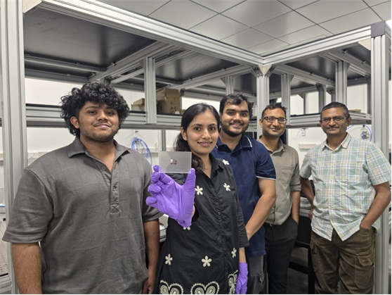
Image: PIB / JNCASR — the research team in the Meta Optics Laboratory (MetoLab), JNCASR, with the fabricated silicon chip used to demonstrate photonic Klein tunnelling (official release image).
Why it matters for India readers
This is Indian public research with a direct line to a technology India will eventually deploy. JNCASR is a Department of Science and Technology institute, and the work sits in the same research current as the country's 6G ambitions: if future networks run on terahertz spectrum, the chips that route those signals will need exactly this kind of low-loss, compact design. The collaboration is also a reminder of how this research gets done — the JNCASR team worked with IISER Kolkata and IIT Bombay alongside partners at A*STAR in Singapore and the University of Lille and CNRS in France.
It also belongs to a wider pattern on this blog's research beat: the recent wins are coming from removing avoidable waste rather than just adding power — see our bistable qubit error-reduction explainer and our 3D Gaussian Splatting partial-updates explainer for two other examples from the same week.
Should you care? ✅ / ⏳
✅ Yes, if you follow chips, photonics or 6G research — a 100 Gbit/s terahertz signal crossing a barrier with 1–2% loss is a genuine building block for on-chip terahertz circuits, and the geometry-based design rule makes it reusable. ⏳ But do not expect it in a phone any time soon: this is a laboratory demonstration, not a commercial chip, and 6G networks themselves are still years away. The next step the team names — tuning the barriers electrically, thermally or mechanically so a device can redirect signals between paths on demand — is what would turn a fixed trick into a switchable circuit.
Price, availability and what is next
There is no price and no product here: this is peer-reviewed research, published in Advanced Materials. Study leader Dr Abhishek Kumar, Assistant Professor at JNCASR, where he heads the Meta Optics Laboratory, put it this way: "Showing that terahertz waves can cross a barrier created simply by changing the hole geometry, while carrying 100 gigabits per second, suggests that this effect can become a useful design tool for terahertz chips." Joint first authors were Samina Mulla and Sangram Kumar Sadhu of JNCASR. What to watch next is the tunable-barrier work — if the team can steer signals on demand, the same chip architecture moves from a demonstration toward a real routing component for terahertz circuits.
FAQs
What are terahertz waves?
Terahertz waves sit in the electromagnetic spectrum between microwaves and infrared light. They offer very wide bandwidth, which is why future 6G networks are expected to use them — but they are hard to guide through compact circuits without losing signal at bends and junctions.
What is photonic Klein tunnelling?
It is the effect demonstrated in this chip: a terahertz wave passes through an engineered barrier in a photonic crystal with almost no loss, rather than being reflected or scattered. Here the barrier is created simply by changing the sizes of triangular holes in the silicon over a short section of the waveguide.
How fast is 100 Gbit/s in real terms?
At 100 gigabits per second, a 5-gigabyte high-definition film could in principle be transferred in under half a second, according to the PIB release. That is a laboratory data rate on a chip, not a consumer internet speed — but it shows the headroom terahertz circuits could offer.
Will this chip be in 6G phones?
Not directly and not soon. This is a research demonstration of a circuit building block, published in Advanced Materials. Commercial 6G hardware is still years away, and a real product would need tunable, switchable versions of these devices — which is exactly the next step the JNCASR team plans to work on.
Takeaway: Indian researchers have shown terahertz signals can cross a barrier on a silicon chip almost loss-free at 100 Gbit/s — a small, reusable piece of the 6G puzzle.
Follow India on TechByCountry for tomorrow's update.
📸 Get tech in the last 24 hours on Instagram — follow @_techinlast24hrs for daily posts (9 AM–9 PM) and reels at 12:30 PM & 8:30 PM.
Sources
Press Information Bureau release (via Technology For You), "Novel silicon chip allowing terahertz waves to pass through barriers could enable future 6G networks" (4 Nov 2026)
Sahyadri Startups, "Terahertz Waves Hit A Wall? This New Silicon Chip Makes Them Pass Through With Just 1–2% Loss!" (4 Nov 2026)
Mulla, Sadhu et al., Advanced Materials (2026), DOI: 10.1002/adma.75322
JNCASR — Integrated Terahertz Photonics (MetoLab research area)
Comments
Post a Comment